Elsyca PCBBalance
The world’s only PCB DFM software that applies automated and optimized copper balancing to your PCB design and panel layout.
More infoDownload file
Elsyca PCBBalance – Future-proofing board and panel plating
A unique solution for PCB designers and CAM engineers
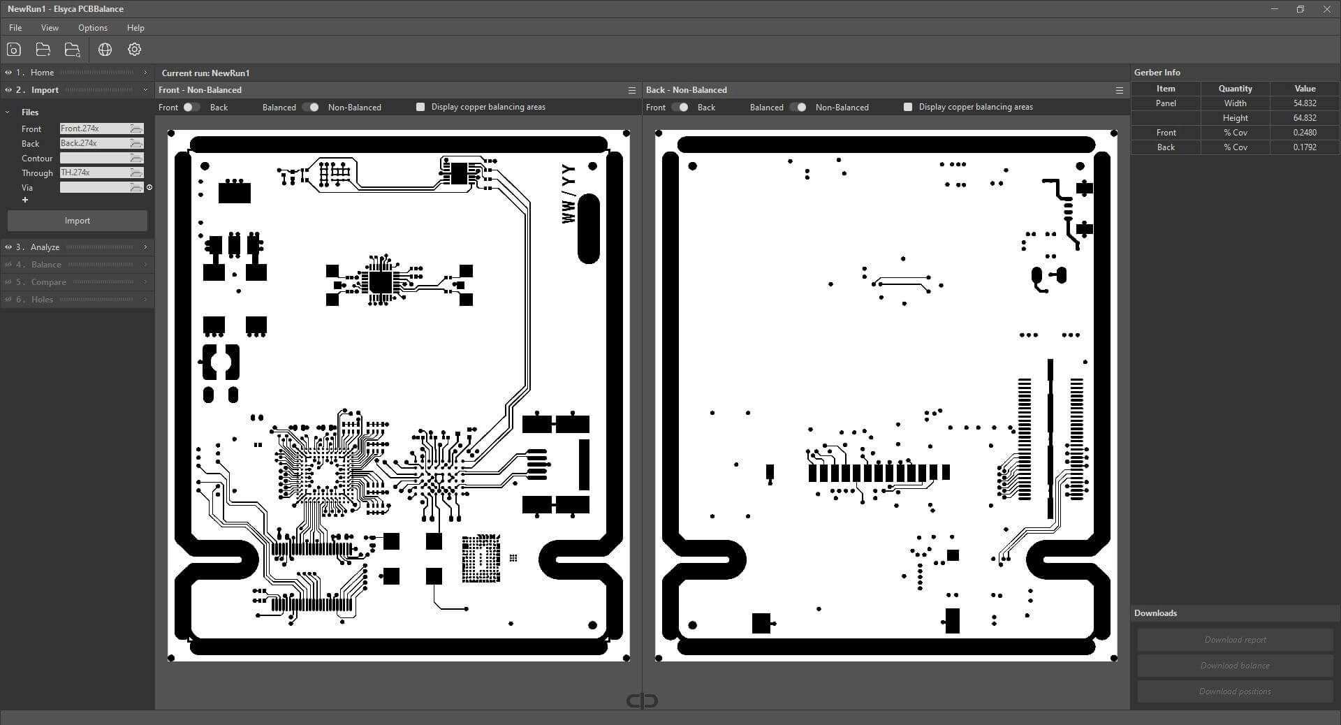
Elsyca PCBBalance is the world’s only software for PCB designers and CAM engineers that not only analyzes the copper layer thickness distribution but also includes an automated copper balancing step to optimize your PCB design and panel layout to prime it for the plating process.
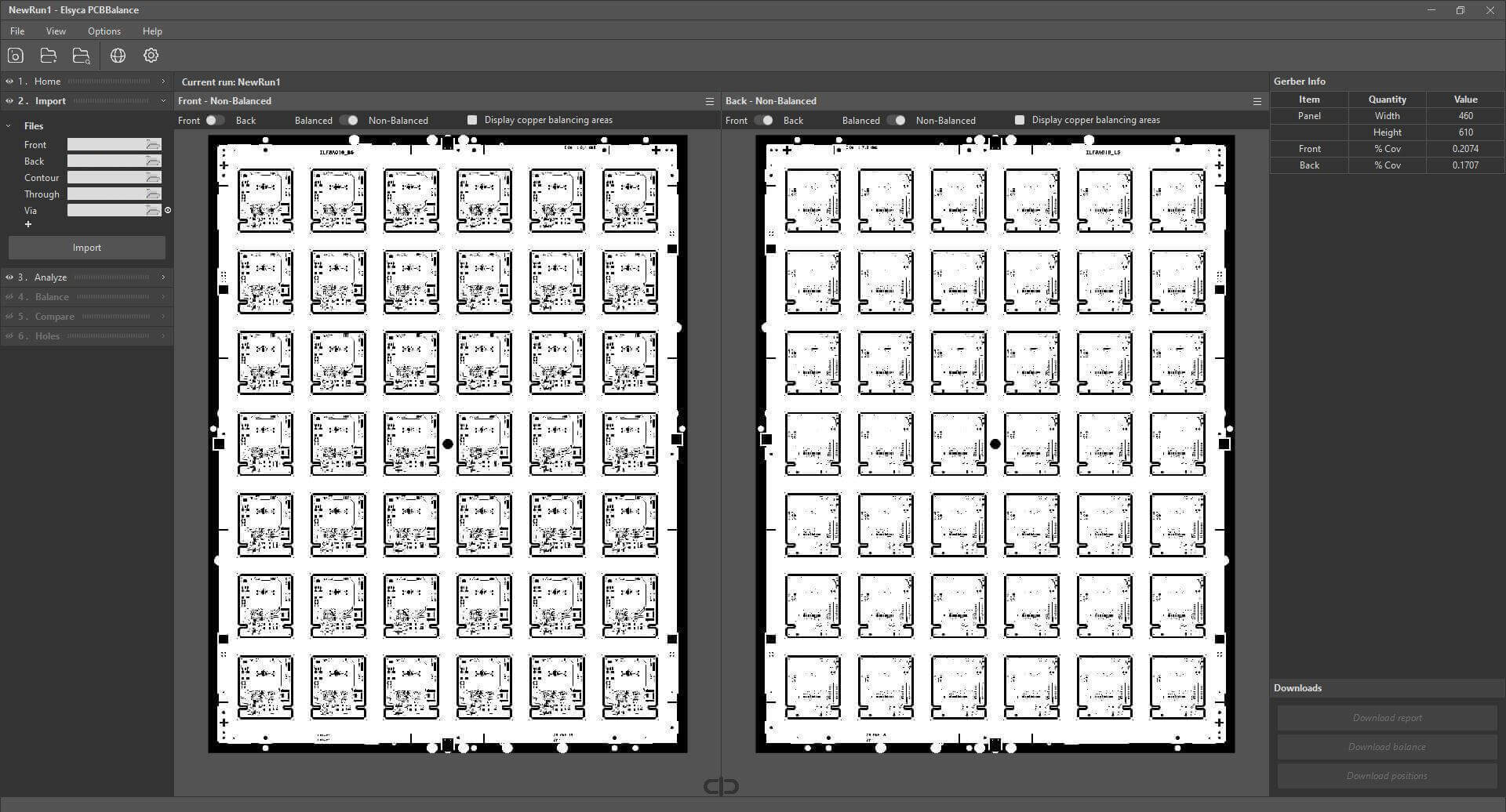
By using Elsyca PCBBalance PCB designers and CAM engineers can evaluate the impact of a specific board or panel layout on the copper plating step during the manufacturing.
Jobs with alternative board or panel layouts can be simulated to compare the plating uniformity and select the optimum configuration. Potential plating issues are identified upfront and mitigative actions can be taken such as modifying the board design/panel layout or launching the embedded single-click balancing algorithm to define the optimal copper balancing layout.
By incorporating Elsyca PCBBalance into the DFM process, the designer, CAM and FAB are assured that the optimal panel layout is submitted for production!


Key Benefits
Quality
Science based automated and optimized copper balancing enables more complex PCB designs and ready-to-plate board layouts. This will reduce the tolerances in production, resulting in higher quality products.
Time & material savings
Manually adding copper balancing easily takes an hour, this software generates one in minutes, and it is an optimal one! This not only saves time in design/CAM departments, it also results in less copper to be plated, resulting in lower material and energy costs
Time-to-Market
No more need to wait for your supplier or production feedback, the software provides immediate input on your design and panel layout.
Knowledge
Understand the impact of your design, and impact of the automated copper balancing
Profit margin
Your profit margin goes up by providing plate-ready PCBs and panels, resulting in higher production capacity and quality products.
Better customer- supplier relationship
As a customer, you will be able to provide FAB products that are easier to plate, as a FAB, you can advise your customer on DFM.
Learn More
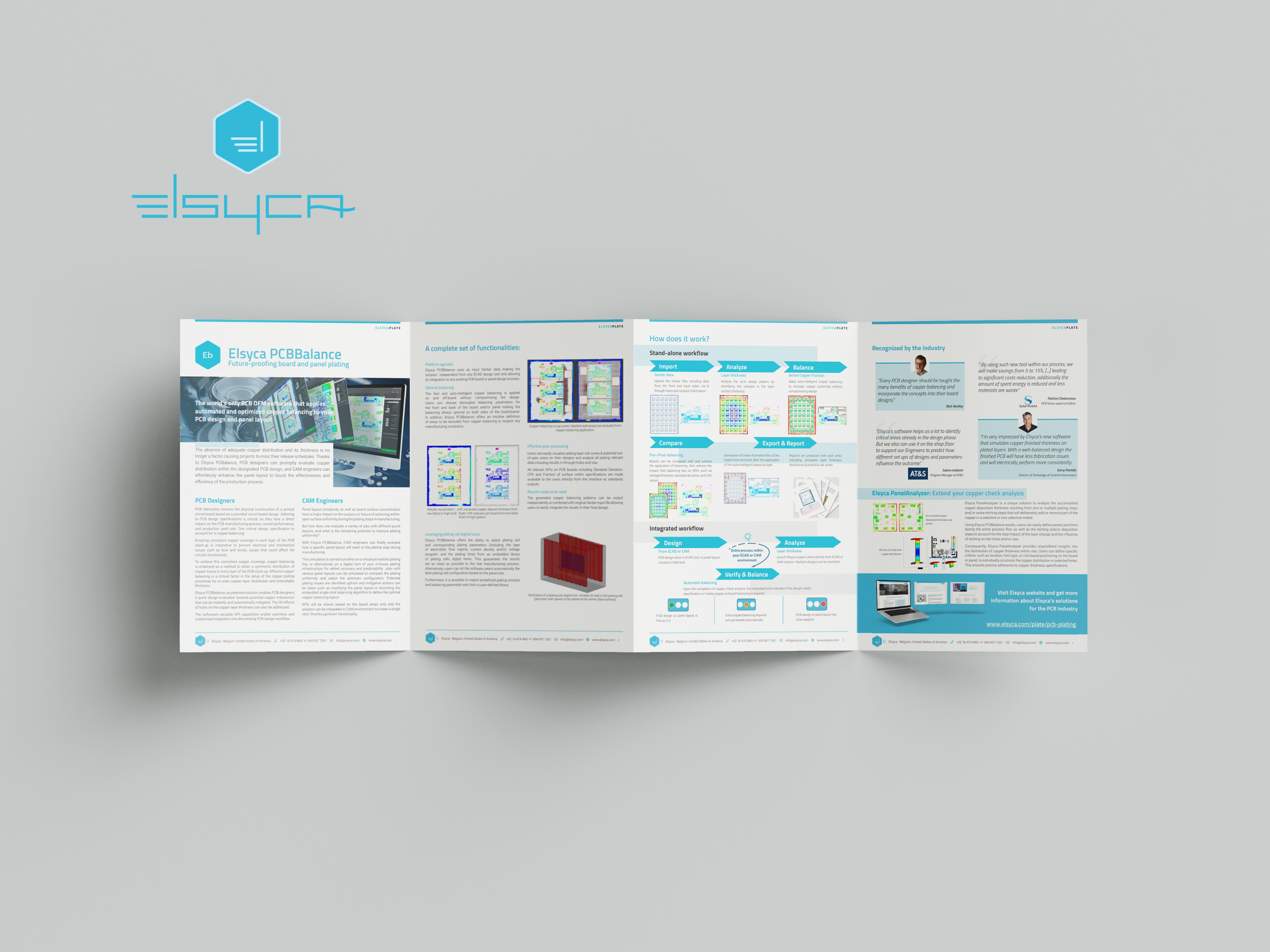
Download file


Key features
A wide range of functionalities

DFM
Understand the impact of your board design and panel layout on the layer thickness distribution with just a few clicks.

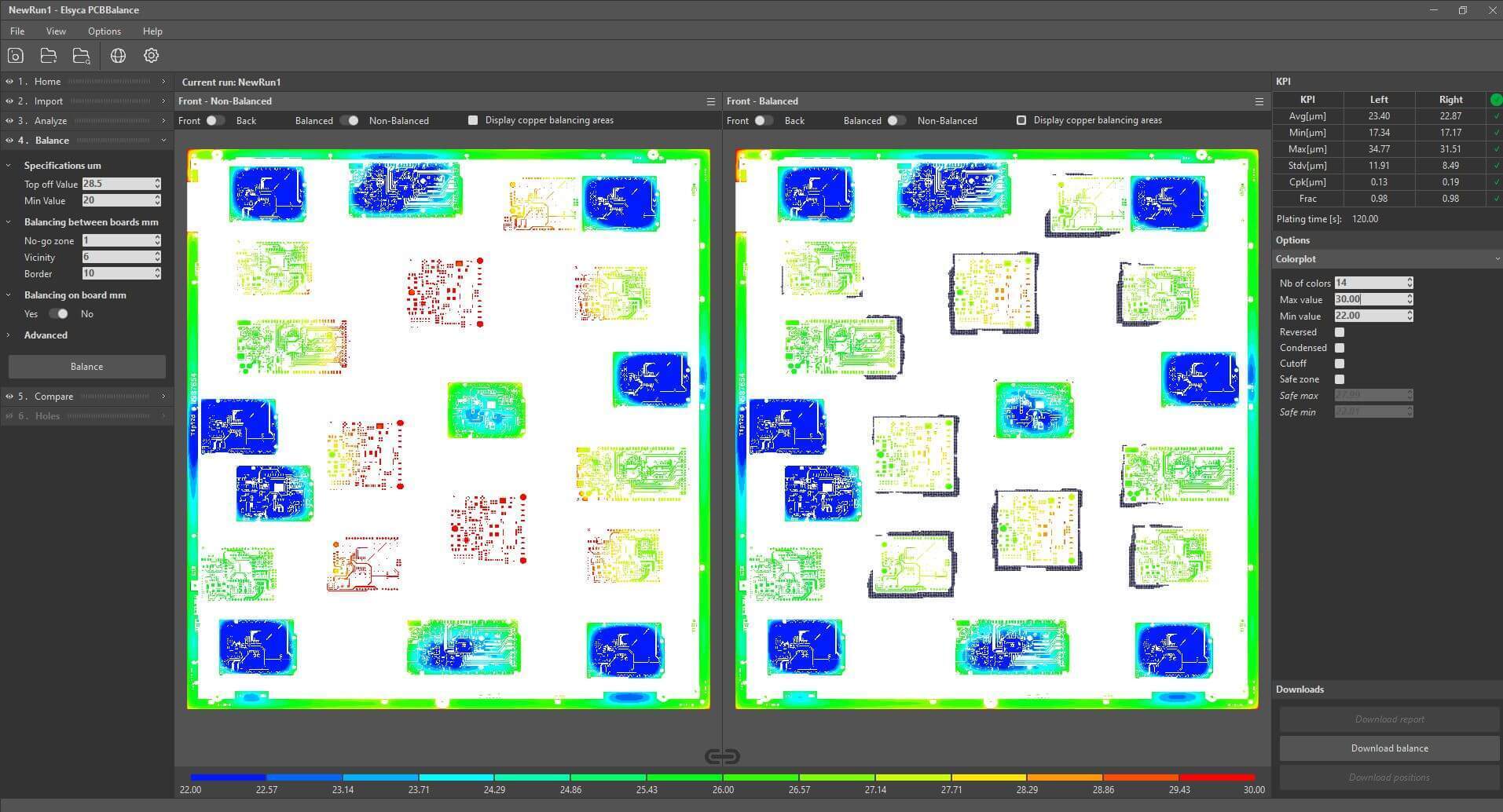
Identify layer thickness distribution over boards and panels
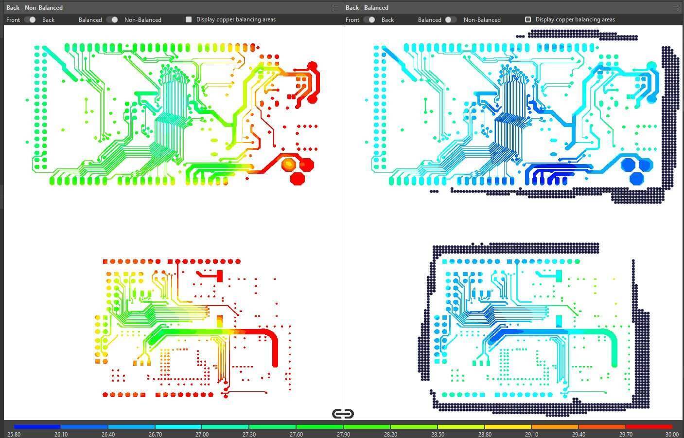
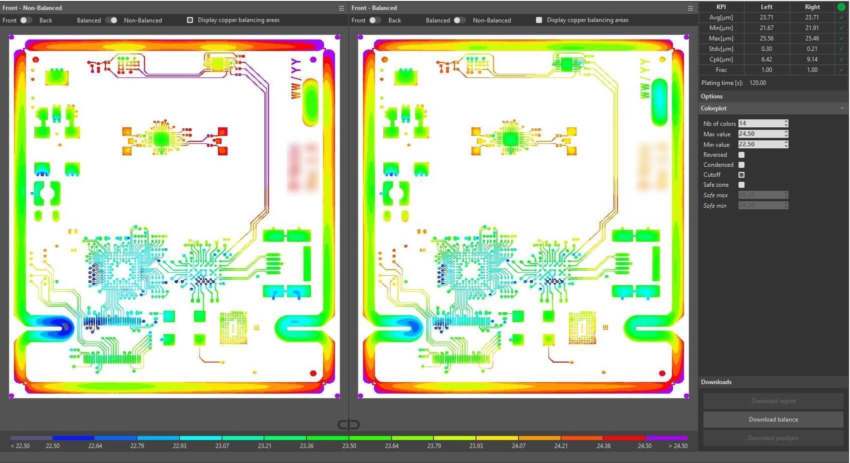
Generate color plots of layer thickness distribution and related production risk zones over the boards and panels.

Automated and optimized copper balancing
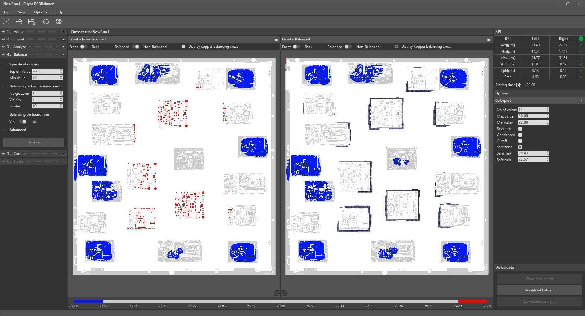
Generate optimized copper balancing with a single mouse click… in only a few seconds time.

Identify the most critical holes for post-production quality testing
Ensure testing is consistent and independent of the operator

Compare different PCB design and panel layouts side by side
Graphical side-by-side views completed with the KPI values provide visual and objective information to select the best design or layout for the plating process.

Download relevant reports
Reports are generated by a simple click in HTML format

Download copper balancing results
Generate extra files in Gerber format containing the exact position and size of the copper balancing locations
Just picture it!
Move the slider
