PCB Plating
Extend your current design and production processes by proven and accurate simulation solutions
Optimize costs, quality, time to market, and production capacity
Ensuring quality throughout the full cycle, from design to production
The entire PCB market is under pressure.
- More components on smaller footprints force PCB designers to use reduced safety margins leading to potential impedance or electrical flow problems;
- FABS are bound by the physics of plating processes while required to deliver high-quality products at the lowest cost in the shortest time possible.
Elsyca's solutions support all the stakeholders involved in the PCB industry by:
- identifying potential quality problems earlier in the process;
- avoiding faulty designs getting into production;
- reducing design iterations for faster time to market;
- ensuring parts are produced to specs;
- qualifying copper layer thickness distribution;
- optimizing production capacity and reduce costs.
Our accurate and fast plating simulation solutions fill the gap between existing tools to ultimately deliver a full quality control over the entire PCB industry chains.
Learn how new predictive engineering modeling solutions are transforming the entire PCB industry.
A key to accelerate the industry shift-left quest to increase product quality consistency.
CAE solutions to extend PCB design and production processes
PCB Designers
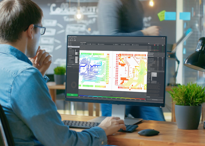
Put PCB design on track for manufacturing success
Upfront DFM check, no need to know any plating or FAB details;
See the impact of your design on copper layer thickness;
Optimize your PCB designs for manufacturing;
Rely on embedded intelligent balancing that outperforms current practices.
CAM Engineers
Create PCB panels that hit the sweet spot between quality and cost
- Make every CAM engineer a plating expert;
- Identify all plating quality hotspots in under a couple of minutes;
- Leverage unique and embedded intelligent copper balancing.
Process engineers
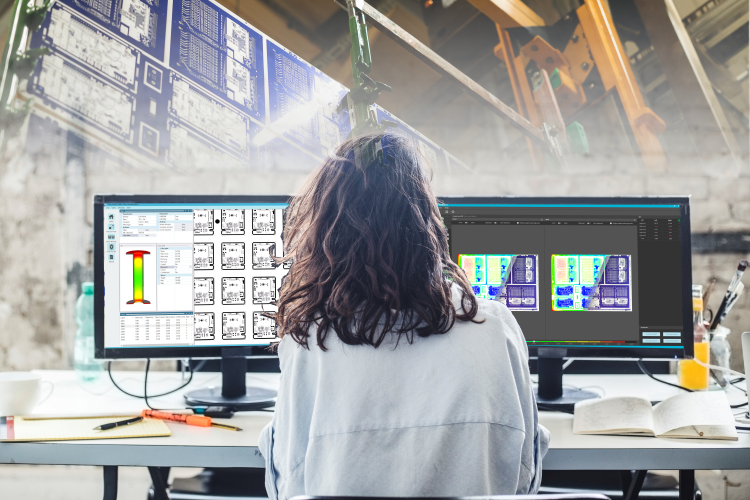
Fine-tune production settings to deliver consistent quality
- Identify and solve plating issues before the first panel is built;
- Identify quality hotspots on the surface and inside holes in minutes;
- Access the final quality information over the entire flight bar.
Controlling the quality at every single step
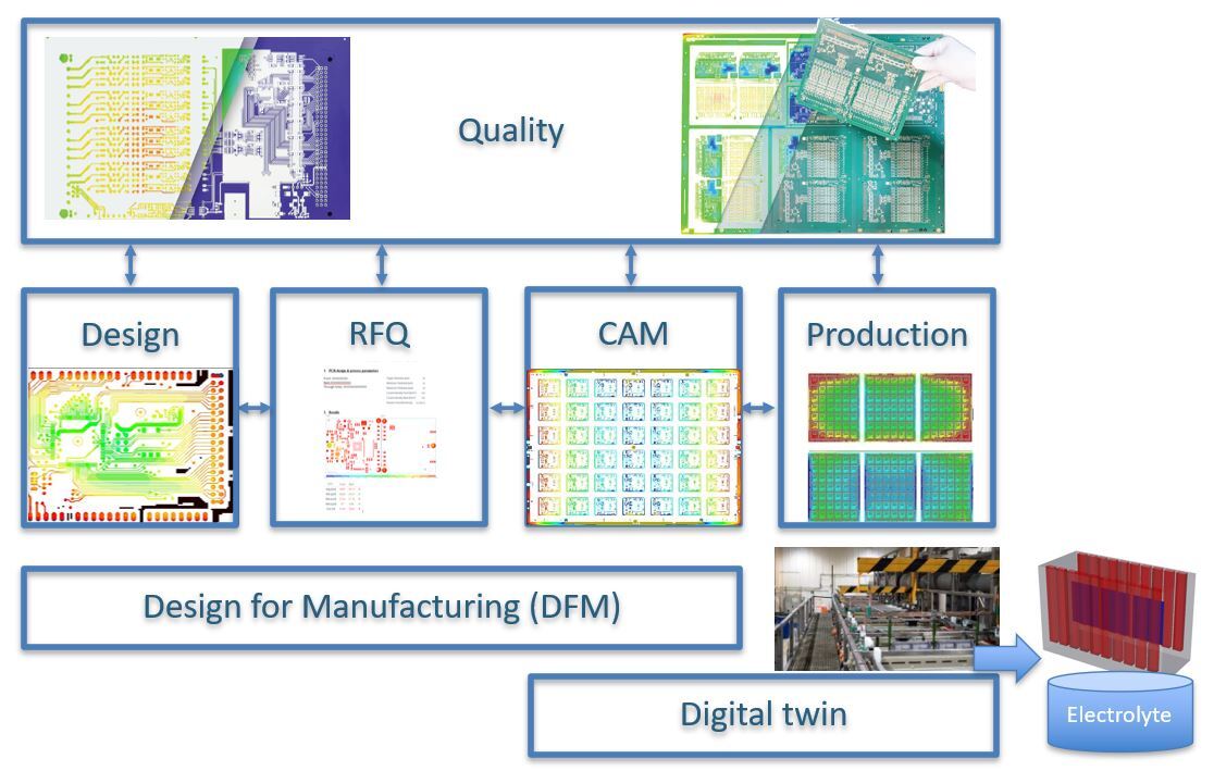
Our solutions for the PCB industry
On the critical importance of considering plating and copper balancing at the design stage
Patrice Chetanneau
PCB Technologies Senior Expert at Safran
As part of the work that we are carrying out with PCB manufacturers and, especially, the French PCB industry, we have understood, more and more, over the last 2 or 3 years, the critical importance of a good copper balancing of the internal and external layers of PCBs, in order to avoid concerns about manufacturing yields and quality, and therefore costs, delays, and raw material waste.
This problem is true for all industries, from consumers to automotive, especially when prices are really tight. Unfortunately, there are not so many designers who are able to understand these issues which are between designer and manufacturer concerns and expertise.
For 8 years, we have worked internally to develop a use of the E-CAD PCB design tool that allows us to do things that are already interesting. But the Elsyca software goes much further, in particular by taking into account the presence of the plating of the vias and holes. We are very interested in this; we would really like to be able to “Elsyca-ize” our PCBs dynamically directly in the PCB design tool.
It is very clear in the interest of E-CAD PCB design tools to offer the integration of such a function because this would allow their customers to pay significantly less for their PCBs, in some cases, savings easily exceeded 10%! (even much more, in certain special cases) and to have much less waste and energy consumption (ecological impact) than one could probably estimate at a few % of the world PCB market (> € 60bn). And given the number of users of E-CAD PCB Design tools, this would have a huge impact on the entire world of electronics, reducing the additional costs and waste generated by imperfect copper balancing !! A great function for E-CAD PCB design tools.
You might also be interested in
Looking for more information?
Don't hesitate to contact us!

